Small
Things Considered Hyuck Choo is a
master of microscale mechanics and miniature movable mirrors.
Massie Santos Ballon takes a close look at the man
and his plans. Illustrated by Joe
Sharkey and Koko
Takatori. 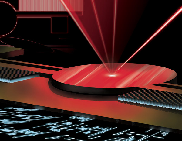
Illustration:
Joe Sharkey Hyuck Choos
second home is a workshop simply known as Room 173. Its behind the
door marked Optoelectronics Lab on the first floor of Cory Hall,
home to the electrical engineers and computer scientists at UC
Berkeley. The boyish postdoctoral researcher
often thought about connecting the workshop to his actual home. If
I could just walk into the lab from the bedroom, that would be OK,
he says. To say Choo used to live in Cory Hall isnt much of an
exaggeration. During the early years of his graduate studies in
electrical engineering, Choo would spend 18-hour days in the building.
He divided his time between Room 173, where he designed and tested
microscale devices, and the MicroFabrication Laboratory on
the fourth floor. There, he made microelectromechanical system
devices, or MEMSincluding some blazingly fast "microscanners"
that could form the heart of an ingenious pocket-sized projector.
A microscanner is a tiny machine with a
movable mirror that directs laser beams. People have made these
devices for nearly 40 years. Anyone whos seen the brief flash of
light when a cashier scans an items bar code at the checkout counter
has seen one in action. And anyone whos used a laser printer or
laser copier can thank microscanners for getting the job done.
Choo, 36, likes to sweat the small stuff. He
and his colleague David Garmire, a computer scientist, patented a
simple and low-cost technique to make microscanners. They're not
the world's smallest, Choo says, but they're "the best ever."
About 90% of the devices work, an unheard-of rate for a university
lab. Scaling the assembly up to a commercial process could pay off
handsomely for the duo. A life of
tiny motors I heard about
micromachines when I was an undergraduate, Choo says. I could make,
actuate, and control tiny little parts that were even smaller than
my hair, and they could still perform useful functions. In some
sense, MEMS is the fusion of advanced science and my childhood
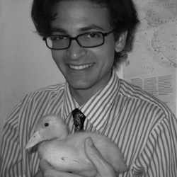
toys. 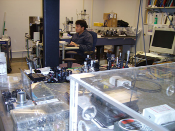 | Photo: Massie
Santos Ballon | | Engineer Hyuck Choo works in the optoelectronics
lab at UC Berkeley. | | |
Under a shock of black hair,
Choo's eyes sparkle as he traces his interest in tiny motorized
devices back to his childhood in South Korea. Lego Technic sets
that let kids build moving things out of blocks, gears, and wheels
were too expensive for the average household there, but Choo remembers
building and playing with remote-control models of tanks and buggies.
Koreans must have toys that are motorized, he says. After moving to America during his teens, Choo
entered the engineering program at Cornell University. There, he
encountered a textbook that changed his life and brought him to
Berkeley. From his bookshelf, Choo pulls
out the dark blue text. Device Electronics for Integrated
Circuits, 2nd edition, doesnt seem like a compelling read, but
the researcher says he often pored over the chapters until the wee
hours. The book introduced him to MEMS technology, he says. When
one of his Cornell professors mentioned that the books author, Richard S. Muller, still
had a lab at UC Berkeley, Choo applied to join it. Muller, founding director of the Berkeley Sensor
& Actuator Center, says Choo brought in new ideas for the
microscanner project his lab had been working on for several years.
He has a very searching mind, says Muller, who is retired. The
idea crystallizes and takes shape, even as hes describing it.
Choo has a knack for keeping it simple, adds
former UC Berkeley collaborator Rishi Kant. The simplicity of
Hyucks solutions makes them easily realizable, says Kant, now a
graduate student at Stanford. Like so much of engineering, MEMS
boils down to problem solving that, he says, is Choo's fort.
A man, a plan, a partnership
Over spring break, David Garmire returns from
his new faculty position at the University of Hawaii, Manoa, to
catch up on projects with Choo. During a pizza lunchcomplete with
Hawaiian slicesthey recall how their partnership began. Garmire met Choo while working in a lab next to
Room 173. Frequent hallway encounters led them to collaborate.
When Choo came up with the idea of working on microscanners, the
computer wizard Garmire was the person he approached. Choo brought
the manufacturing savvy, while Garmire excelled at software and
testing. I wouldnt have pursued it without
David, Choo says. If you just demo the microscanner fabrication,
the work only has half the value. The fabrication and device
testingthat was possible because we worked together. Ive found Hyuck to be more than an engineer, Garmire
says in response. He is someone who cares strongly for his family
and community, has a deep understanding of history, and is a great
friend. Garmire, 29, looks like a curly-haired
blond teenager next to the stocky Choo. His interest in computer
science started as a kindergartener playing with his fathers
calculator. By high school, he was writing code and programming
in a number of computer languages. My heart was set, he says. I
was fascinated by the fact that you could recreate physics on a
computer and predict what happens in the real world from the simulated
world. The two researchers have big plans
for their microscanners. Their business plans for making the
microscanners won awards at various competitions. Now theyre working
on bringing the key element to fruition: producing laser modules
for pocket-sized projectors. It's a long
journey that starts in Room 173. For the benefit of a visitor,
Choo agrees to simulate the entire fabrication process. He starts
at his computer, clicking on file icons around desktop images of
his son, to pull up diagrams of a microscanner. They're rectangular
schematics in various colors, each corresponding to a layer on the
device. On the screen they loom large and garish, but the finished
product will be smaller than a square centimeter.
 | Photo: Courtesy of Hyuck Choo |
The tiny mirror
in this microscanner, made at the UC Berkeley MicroLab, pivots
thousands of times each second. | |
| Lines and curves
indicate the locations of the tiny mirror. Rows of bars depict
miniature combs that allow the mirror to pivot back and forth,
directing the lasers movements in precise patterns. Two sets of
combs with overlapping teeth bracket a thin band that centers the
mirror. Electrical impulses drive the comb attached to the band;
the other comb is fixed in place. The
diagrams dictate the fabrication process, in which the device's
layers are etched with chrome onto three thick quartz glass plates
called photolithography masks. These masks will transfer the designs
onto silicon wafers to make the microscanners in the magical workshop
where Choo says all the grown-up toys are made: the campus MicroLab.
Going through the motions
The key to using the MicroLab is preparation.
Every minute inside costs 50 cents, and that quickly adds up during
the time-consuming work. Choo admits that he learned to come in
with a plan after a few time-and-money-consuming blunders during
the first year he used the facility. To run
through a mockup of the microscanner fabrication process, Choo first
needs to dress for entry. The MicroLab is a Class 100 cleanroom,
meaning there shouldnt be more than 100 particles greater than 0.5
microns in size within each cubic foot of air. In comparison, a
human hair is a whopping 100 microns thick. Every time Choo moves,
he sheds particles. So to enter the MicroLab, he must don a blue
shower cap, safety glasses, gloves, white Tyvek coveralls, blue
shoe covers, and white Uggs-like Tyvek boots. It
takes Choo less than a minute to gown up except for the gloves and
boots. Ive had practice, he says simply. He
steps around a bench that separates the dirty and clean gowning
zones and onto a sticky mat before covering his hands and feet.
Its a short walk from there to the lab, where Choo opens the door.
A persistent buzz of white noise instantly bombards the senses. In
the first step of his simulated demonstration, Choo bakes a layer
of photoresistant liquid onto a silver, four-inch-wide silicon
wafer. Disc in hand, he crosses a corridor to a machine that will
imprint each photomasks design onto the wafer. With the first
design down, he heads to a room housing the silicon etcher. In a
four-hour process, the machine would etch the areas on the silicon
wafers that are not covered by the photoresist-imprinted pattern.
Then, a machine resembling an ancient dot matrix printer would
verify that the desired etching depth was achieved. Choo would repeat the imprinting and etching process
twice more on the front and back of the silicon wafer. A single
4-inch wafer could yield 116 microscanners, neatly arrayed across
the face of the disc. After all this work, the etched squares of
mirrors and combs are barely visible, almost looking like outlines
rather than three-dimensional objects. They sit just 50 microns
above the wafers surface. To cut them out,
Choo walks through wooden doors to a small room with a dicing
machine. Here the buzzing noise pervading the MicroLab gives way
to a high-pitched hum, reminiscent of sci-fi shows from the 1960s.
The wafer goes under the microscope, its image enlarged on the TV
screen above. Crosshairs on the display allow Choo to line up the
wafer's image with the boundaries of its intended design before he
makes any cuts. With the cut microscanners
temporarily bonded onto a blank wafer for easy portability, its
time for a fourth and final run through the silicon etcher to free
the movable combs that will allow the mirror to twist. An acid
bath removes the finished scanners from the wafer; one final machine
blasts carbon dioxide gas to dry the devices. In
Choo's whirlwind walkthrough of the MicroLab, this all took an hour.
Doing it for real, though, takes two weeks. And thats short, Choo
notes. Current commercial applications can take up to six months
to make microscanners, he says, drastically increasing the production
costs. At this point, Choo would hand the
finished microscanners off to Garmire for testing. When assembled,
the Lego-like pieces of circuitry are about an inch long, with the
mirrors nestled at their centers. Testing them involves connecting
both the microscanners and a tiny laser beam to a computer program
that Garmire wrote. Making accurate measurements with such small
structures, he notes, is tricky. First,
Garmire verifies that each microscanners mirror resonates at the
desired frequency. By changing the voltage that goes through the
attached combs, he can change the speed at which the mirror swivels.
It's generally faster than the eye can see: Choo has a video showing
a mirror pivoting 7,800 times per second. Some of their scanners
are designed to move three times faster than that. To check on the accuracy of these micromovements,
Garmire sends a burst of laser light to the tiny device and then
measures how much of the light gets deflected by the mirror.
He refines and adjusts the angles as needed to ensure that the laser
targets the right area of the mirror every time. When everything
works smoothly, the mirrors can steer laser light, allowing them
to scan surfaces rapidly, form any pattern desired for use in
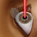
applications such as refractive eye surgery (see
sidebar) and even project moving pictures. The
efficiency of the team's process, start to finish, has impressed
outside observers. Yields of 70 to 90% are very high for a university
lab, says Olav Solgaard, an electrical engineer at Stanford.
Those numbers mean that commercialization might be easier and more
profitable than for many earlier MEMS structures that are difficult
to make in a commercial foundry. Green will mean go
Choo and Garmire want to mass-produce modules
that contain their microscanners, laser light sources, and electronics
to control the lasers for a low-cost portable projector. It would
be a true pocket device, the size of a cell phone, rather than the
tabletop projectors now in vogue in most classrooms and boardrooms.
But the technology still faces a few barriers. Notably, the modules must contain three colored
lasersblue, red, and greento combine their images into full color
for our eyes. Think of having 3 laser points sweeping across a
screen really, really fast, Garmire says. To handle these bursts
of color, each module would contain up to six independently controlled
microscannerstwo mirrors per laser. However,
only the red and blue lasers are now available in semiconductor LED
diode forms. Choo seems willing to wait a couple of years for
companies to develop a green laser diode. When I was an undergrad,
he says, the blue laser diode was just a dream. Now it has a
lifetime of 10,000 hours. In the meantime,
Choo still plans to work on other MEMS projects in Room 173. But
he has a new and even more exacting pursuit now: He has joined a
nanotechnology lab at Lawrence Berkeley National Laboratory's Molecular Foundry, just up the hill from UC Berkeley.
There, he'll set his sights on creations 1000 times smaller than
the microscanners that consumed so many of his years. Choo won't be bringing his work home though. The
9-to-5 man has a different kind of miniature projecthis
three-and-a-half-year-old sonwaiting for him there with plans of
his own. Soon there will be two voices bossing the researcher
around; another child is on the way. He
specifically tells me what to do, Choo grins. We play pirates,
ride bikes, or play with his toys. He has Legos! From
the gleam in Choo's eyes, its not clear who enjoys the plastic
bricks more. Top
Sidebar: The Light in Your Eyes
As graduate students at UC
Berkeley, Hyuck Choo and David Garmire thought their optical
microscanners were ideally suited for refractive eye surgery. They
demonstrated a system that Garmire describes as good as the state
of the art. The challenge is steep: A
microscanner used in surgery must be so accurate and stable that
it slices exactly the right tissues, every time. We dont want to
blind somebody, Garmire observes. Laser
control is crucial, agrees Dr. Danny Lin, a surgeon with the Pacific
Eye Associates in San Francisco who works with two different types
of laser systems. The location, depth, power, and proximity of the
laser applications need to be exact. Dr.
Todd Severin, medical director of the Pacific Laser Eye Center
Medical Group and a surgeon at UC Berkeleys Refractive Surgery
Center, concurs that keeping the laser on target is tricky. What
youre trying to compensate for are the little psychotic movements,
he says. A lot of patients vibrate. When youre working within a
6.5-millimeter zone, one millimeter is a huge movement. Garmire says their microscanners deal with such
eye movements by moving faster than the eye can. Monitoring the
patients eye movements allows the surgeons to time the laser pulses
that ablate the eyes surface. Feedback systems keep the mirrors
oscillating at stable speeds. This reduces the possibilities of
errors occurring during surgery and shortens the amount of time a
patient must wait for the eye surgery to be complete, Garmire
says. As the researchers pursued popular
applications for their microscanner patent, Garmire and Choo shifted
their focus to developing pocket-sized projectors. However, they
havent forgotten the promise of the original eye surgery proposal.
We think people will find both applications highly useful and
beneficial, Choo says. Top
Biographies Massie
Santos Ballon
B.A. (molecular biology and
biochemistry)
Wesleyan University
Internship: 23andMe
(Mountain View, CA) What are you doing next?
was the question from my biology professor. Most of my lab colleagues
looked ahead to graduate school or medical school, but I talked
about teaching English literature to Filipino college students. My
professor's shock mirrored the reaction three years earlier of my
high-school English teacher, who was amazed to learn I was a science
major. But for me, creative writing always
complemented the hands-on lab work. Science was more fun when I
could write and talk about research outside of my dry lecture
courses. Ive tried to share that delight as a science columnist,
technical writer, textbook coauthor, and even in a literary contest.
Although many people think understanding science is as intimidating
as appreciating poetry, Im working on proving them wrong. . . . . . . . . . . . . . . . . .
. . . . . . . . . . . . . . . . . . . . . .
. . . . . . . . . . . . 
Joseph C. Sharkey
B.A.
(Visual Arts), University of San Francisco I have been drawing and flipping rocks in search
of creepy-crawlies since my earliest days in San Jos. Hoping to
better the world through visual communication, I studied graphic
design, education and variety of visual media in San Francisco.
I am intrigued by the educational potential of the synthesis of art
and science, as both are excellent methods through which we can
learn about our world and ourselves. The challenge of focusing my
artistic process toward scientific communication has been truly
thrilling. I hope to use my training in science illustration to
educate people about the wonders of the natural world, inform about
issues of environmental justice, and help make science accessible
to everyone. My scientific interests are evolution, botany,
herpetology, ecology and climate change. I will soon be completing
illustrations for a natural history guide to Mojave Desert birds.
. . . . . . . . . . . . . . . .
. . . . . . . . . . . . . . . . . . . . . .
. . . . . . . . . . . . .  Koko
Takatori Koko
Takatori
B.A. (psychology, pre-medicine)
Wellesley College
I was
born in Tokyo, Japan, where I attended international schools. My
high school AP art course was where I realized my passion for
visualization. I graduated from Wellesley College in 2007, where
I took core science courses as a pre-med. Unable to let go of my
passion, I entered the Science Illustration Program, which fused
the two fields of study that I love. Currently, I am interning at
a 3D medical animation studio in New York City. Top |